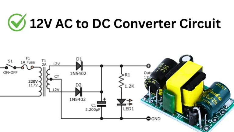
Do you want to build a simple variable power supply for your electronic project. The LM317 Variable Voltage Regulator Circuit is easy to build and it will converting the high DC input voltage to adjustable lower output voltage. The circuit diagram, working explanation and other important details are given in this article. This project cost is very less comparing with any other converter devices buying from the market.
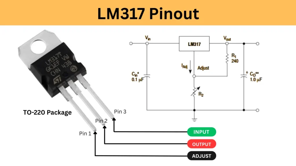
LM317 Voltage Regulator Pinout
Components Required
| Component | Value/Part Number | Description |
|---|---|---|
| IC1 | LM317 | Adjustable Voltage Regulator IC |
| D1, D2 | 1N4007 | General-purpose Diodes (reverse protection) |
| R1 | 220Ω | Resistor (fixed) |
| R2 | 1kΩ | Resistor (fixed) |
| P1 | 5kΩ | Potentiometer (for voltage adjustment) |
| C1 | 100µF / 50V | Electrolytic Capacitor (input filtering) |
| C2 | 100nF | Ceramic Capacitor (input stability) |
| C3 | 10µF | Electrolytic Capacitor (output stability) |
| C4 | 100µF / 50V | Electrolytic Capacitor (output filtering) |
| J1 | DC IN Connector | 2-pin screw terminal (input voltage) |
| J2 | DC OUT Connector | 2-pin screw terminal (for variable output) |
| PCB or Breadboard | – | For assembling the circuit |
| Heat Sink | For LM317 | Recommended if output current > 500mA |
Circuit Diagram
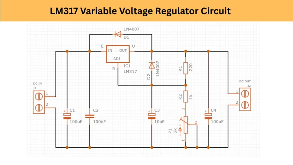
Circuit Connection
In the give diagram of LM317 variable voltage regulator circuit, the input voltage is connected to the IN connector mentioned as (J1). The positive terminal is connected to both 100uf capacitors of C1, and C2. This capacitor is used as an input filtering and noise suppression. This filtered voltage is then goes into the Dc voltage Input pin of the LM317 voltage regulator.
The OUT pin of the LM317 provides the regulated output voltage, which is connected to both a protection diode (D2) and capacitor C3 (10µF) to improving the stability and prevent reverse voltage. The adjustable voltage output is set using a resistor voltage divider by R1 (220Ω), R2 (1kΩ) and a 5kΩ potentiometer (P1) connected between the output and the ADJ pin of the LM317.
This configuration is using to tuning of the output voltage. The final output passes through capacitor C4 of 100µF for additional filtering. Diode D1 is placed in reverse across the input and output to protect the regulator IC from reverse current damaging, especially when the input supply is disconnected while the output capacitor is charged. This circuit ensures a smooth, adjustable, and safe DC output and it is suitable for a wide range of electronic applications.
Working of Variable Voltage Power supply
The LM317 regulator circuit is working using LM317 IC. this circuit maintaining the stable voltage in output either the input voltage is slightly fluctuated. The input DC voltage is filtered by the capacitors C1 and C2 before goes into the input pin of the LM317.
In the internal circuit of the IC reference voltage is 1.25V and it is maintained between the OUT and ADJ pins. By using a combination of fixed resistors (R1 and R2) and a variable resistor (P1) the voltage divider is formed and that will adjusts the voltage at the ADJ pin, so this will changing the output voltage.
The output voltage is calculated by using the formula of Vout = 1.25V × (1 + R2/R1) Iadj × R2
The Capacitor C3 will enhances the voltage stability and C4 smooths the final output. Diodes D1 and D2 provide reverse polarity and discharge protection. This configuration is very safe, smooth and perfect for powering various electronic circuits.
Applications
- Adjustable DC power supply
- Battery charger
- Bench power supply
- Voltage Regulation in DIY Electronics Projects
- Power Supply for Audio and RF Circuits
- Automotive Applications